K1 Semiconductor Joins Chicago Quantum Exchange to Enhance Wafer Reuse
Chicago, Thursday, 14 August 2025.
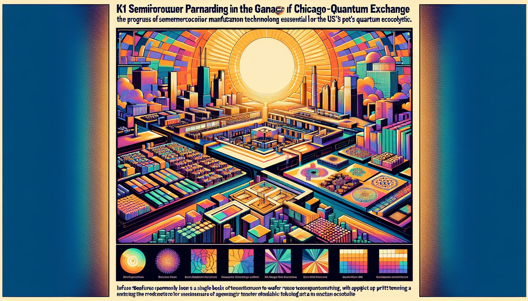
K1 Semiconductor partners with Chicago Quantum Exchange to enhance wafer reuse technology, highlighting the advancement of semiconductor manufacturing vital for US’s quantum ecosystem.
The Significance of Wafer Reuse
K1 Semiconductor’s partnership with the Chicago Quantum Exchange (CQE), officially announced on August 12, 2025, represents a strategic move towards improving wafer reuse techniques in semiconductor manufacturing. This collaboration places a spotlight on the critical role of sustainable technologies in the advancement of the United States’ quantum computing capabilities. By joining forces with CQE, K1 Semiconductor aims to develop high-performance semiconductor materials that can be reused up to 20 times, providing a significant reduction in material costs and environmental impact [1].
The Role of Photonics in Semiconductor Advancements
Photonics technology, which utilizes light instead of electrons for signal processing, plays a vital role in this collaboration. By integrating photonic elements into semiconductor devices, there are potential benefits such as reduction in power consumption and improvement in data processing speeds. This technology is particularly essential in quantum computing applications where minimizing optical losses is crucial for performance efficiency. K1 Semiconductor’s innovations in wafer processing techniques, including their advanced polishing and integration methods, aim to minimize these optical losses, thereby enhancing the efficiency of photonic circuits [2][3].
Implications for the Global Electronics Sector
The implications of this collaboration extend beyond the U.S. borders, especially for electronics sectors in countries like South Korea, Japan, and Singapore. These regions, known for their leading roles in semiconductor and electronics manufacturing, might witness similar innovations as they look to capitalize on the advancements in wafer reuse technologies. The ability to significantly reduce manufacturing costs while maintaining high precision opens the door for more accessible and sustainable solutions in the global electronics industry. This can have a ripple effect, energizing the industry’s supply chains and fostering more collaborative initiatives across borders[1][2].
K1 Semiconductor’s Growing Influence
K1 Semiconductor has already established itself as a burgeoning force within the semiconductor industry. The start-up, co-founded by students from the University of Chicago’s Pritzker School of Molecular Engineering and the Booth School of Business, demonstrates how academia and industry collaboration can drive technological progress. By leveraging the CQE’s ‘Founder Platform,’ K1 is set to access vital resources, including advanced research infrastructure and partnerships with companies like Great Lakes Crystal Technologies, further bolstering their efforts in quantum sensing technology [1].
Future Prospects and Strategic Directions
As K1 Semiconductor continues to make strides in the semiconductor landscape, the company’s strategic focus on sustainable manufacturing and photonics positions it as a key player in the U.S.’s endeavor to establish a self-sufficient quantum technology supply chain. This also aligns with global efforts to advance photonic technology, an area expected to see substantial growth as industries seek to reduce energy consumption and enhance computing capabilities. The CQE partnership not only marks a step forward for K1 but also symbolizes a broader shift towards innovation-led growth in quantum computing [1][2][4].